This article will examine various layout strategies for GaN FETs, analyzing how different PCB configurations affect added resistance for each design.
This article is published by EEPower as part of an exclusive digital content partnership with Bodo’s Power Systems.
With the advent of next-generation GaN transistors operating in the 40 V to 15 V range, RDS(on) specifications have reached the remarkable level of hundreds of micro-ohms (as illustrated in Table 1), significantly outperforming comparably-sized power MOSFETs. To fully capitalize on the advantages of these ultra-low resistance FETs, careful PCB layout is essential to prevent any additional resistance that could undermine their performance.
Table 1. Seventh generation GaN transistors in QFN packages from Efficient Power Conversion (EPC) have RDS(on) as low as 280 micro Ohms
|
EPC2373 |
EPC2370 |
EPC2371 |
EPC2372 |
EPC2366 |
EPC2374 |
|
|
BVDSS |
15 V |
15 V |
25 V |
25 V |
40 V |
40 V |
|
ID (cont) |
88 A |
101 A |
88 A |
101 A |
88 A |
101 A |
|
ID (pulse) |
447 A |
783 A |
412 A |
699 A |
360 A |
553 A |
|
RDS(on) typ |
0.47 mΩ |
0.28 mΩ |
0.65 mΩ |
0.37 mΩ |
0.8 mΩ |
0.5 mΩ |
|
QG typ |
18 nC |
31 nC |
17 nC |
27 nC |
13 nC |
24 nC |
|
QGD typ |
1.5 nC |
1.5 nC |
2 nC |
4 nC |
2.1 nC |
3.6 nC |
|
QOSS typ |
17 nC |
29 nC |
18 nC |
29 nC |
20 nC |
34 nC |
|
RΘJC |
0.6 °C/W |
0.5 °C/W |
0.6 °C/W |
0.5 °C/W |
0.6 °C/W |
0.5 °C/W |
|
Device Size mm2 |
2.6 X 3.3 |
3.3 X 3.3 |
2.6 X 3.3 |
3.3 X 3.3 |
2.6 X 3.3 |
3.3 X 3.3 |
QFN Packages for High Power Density
EPC has developed two new QFN packages, illustrated in Figure 1, optimized for both thermal and electrical efficiency. With the rapid advancements in GaN technology, the device’s RDS(on) has become so low that it is essential to ensure that the copper traces and vias on the underlying PCB do not inadvertently contribute to system power losses. To address this concern, we modeled various PCB designs and assessed the additional resistance introduced by the PCB structure itself.
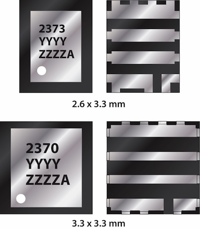
Figure 1. EPC’s new QFN packages featuring dual-sided cooling and optimized copper lead area for PCB attachment. Image used courtesy of Bodo’s Power Systems [PDF]
Modeling Methodology
The resistance of the printed circuit boards (PCBs) was evaluated using finite element analysis (FEA) in COMSOL Multiphysics. PCB and package geometries were imported directly from Altium and 3D CAD models respectively. To reduce computational cost when analyzing the large number PCB variants, the imported layout was restricted to extend only one millimeter beyond the package footprint of the mounted packaged die.
To represent the GaN FET, a rectangular conductive sheet was added to the modeled geometry and connected to the imported package. The sheet’s conductivity was adjusted such that its resistance matched the RDS(on) of the actual device. Additionally, vias imported from Altium appeared as perfect cylinders, which do not accurately capture the plated copper cross-section present in fabricated boards. To account for this discrepancy, the conductivity of the via domains was reduced by 60%, thereby approximating their effective electrical performance.
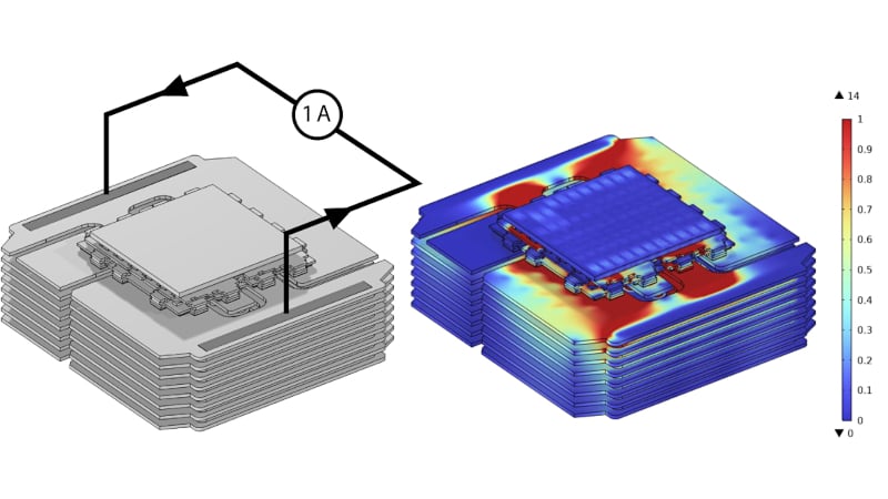
The boundary conditions for the models were defined as follows: a terminal boundary condition was applied to the top surface of the drain input pad (as shown in Figure 2), where a 1 A current source was introduced, and a ground boundary condition was applied to the top surface of the source contact pad to complete the circuit.
To isolate different contributions to the overall resistance, the analysis was segmented into three components: PCB resistance, package resistance, and die resistance (modeled as the conductive sheet). The resistance of each domain was calculated from the volumetric integration of the electromagnetic loss density, normalized by the square of the applied current. This approach enabled clear separation of the resistive contributions from the PCB, package, and device.
Simulation Cases and Results
To cover a broad range of solutions we modeled PCB configurations ranging from single-layer to 16-layer boards with various via densities and inner-layer geometries. Table 2 summarizes these design cases and the resulting PCB resistance for each package. Figures 3 through 5 provide cross sections of the stack-up and other PCB details of all the cases simulated.
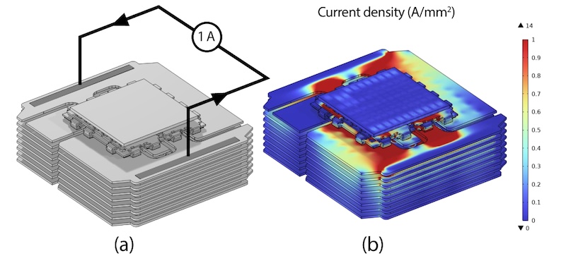
Figure 2. (a) Isometric view of the COMSOL simulation model showing the GaN FET and PCB geometry. (b) Example simulation (8L_Board) output illustrating current density distribution. Image used courtesy of Bodo’s Power Systems [PDF]
In the first study, five cases with different numbers of layers were analyzed to quantify the impact on PCB resistance. The first four use a high number of vias and an interdigitated layout. Figure 4.a (left) shows a top view image with the location of the vias and the layout of the top layer, also repeated on all the inner layers.
Figure 4.b shows the layout of the fifth case, a 16-layer board with HDI technology using blind and buried vias. As expected, the results show that the lowest PCB resistance is achieved with the highest layer count and HDI technology. However, the improvement as the number of layers increases is small beyond eight layers due to the increased resistance encountered by the current as it travels vertically through the vias to spread into the deeper layers.
To understand the impact of vias in PCB resistance, a second study was conducted where the same 16-layer stack-up and interdigitated layout were combined with different via densities. Three via densities were analyzed: high (0.5 mm clearance, Figure 4.a left), medium (0.75 mm clearance, Figure 4.a center), and low (1 mm clearance, Figure 4.a right).
The conclusion from this study is clear; to fully utilize all the layers, a high via density is required. Otherwise, even the 16-layer board with a medium via density yields a higher PCB resistance than an 8-layer board with high via density.
Table 2. Summary of the cases simulated and corresponding results.
|
PCB Stack-up |
# of Vias |
Inner layer design |
Package (mm x mm) |
||
|
2.6 X 3.3 |
3.3 X 3.3 |
||||
|
Simulated PCB Resistance (µΩ) |
1L_Board |
High |
Interdigitated |
269 |
307 |
|
4L_Board |
131 |
139 |
|||
|
8L_Board |
101 |
103 |
|||
|
16L_Board |
93 |
93 |
|||
|
16L_Board_HDI |
82 |
84 |
|||
|
16L_Board |
High |
Interdigitated |
93 |
93 |
|
|
Medium |
107 |
107 |
|||
|
Low |
119 |
119 |
|||
|
8L_Board |
As allowed by design |
Interdigitated |
101 |
103 |
|
|
Split planes |
104 |
106 |
|||
|
Interleaved |
126 |
131 |
|||
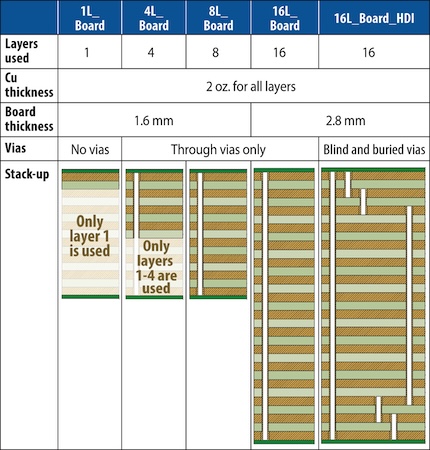
Figure 3. Cross-sectional views of the representative PCB stack-ups studied. The far-right example demonstrates a high-density interconnect (HDI) structure, while the others employ conventional throughvias. Image used courtesy of Bodo’s Power Systems [PDF]
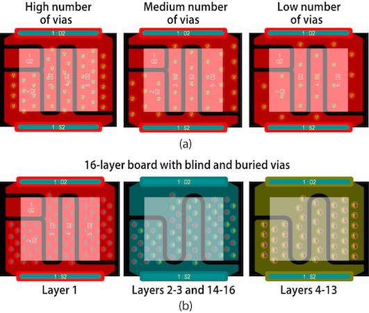
Figure 4. (a) Top view of the layout showing the via densities analyzed. (b) Top view of the 16-layer board with HDI technology showing the placement of blind and buried vias. Shadow represents GaN die placement. Image used courtesy of Bodo’s Power Systems [PDF]
Finally, a third study was conducted to evaluate the layout used in the inner layers. Figure 5 displays the three alternatives considered. The first variant (Figure 5.a) uses an interdigitated layout repeated on all layers. The second variant (Figure 5.b) uses a split plane design where half the area under the device is dedicated to the drain or source terminals in all the inner layers.
Both the interdigitated and split plane variants use the same high via density and the performance is very similar, with a slight penalty for the latter one. The third layout variant uses an interleaved design with medium via density where even-numbered layers are dedicated to the source and odd-numbered layers to the drain.
The larger spacing between the vias creates conductive channels between them that increases the effective cross section on each layer. Nevertheless, the negative impact of a smaller number of vias and the fact that each terminal is only present on half the number of layers, overwhelms any of the benefits.
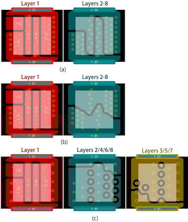
Figure 5. Top view with various layout designs (a) interdigitated planes for drain/source on all layers, (b) split drain/source planes on all inner layers, and (c) interleaved drain/source layers. Image used courtesy of Bodo’s Power Systems [PDF]
It is worth noting that the PCB layout must balance resistance minimization with other design considerations when integrated into a full converter solution. For example, in a buck converter parasitic inductance introduced by inadequate layout could have a negative impact on performance [1].
Findings and Guidelines
Table 3 shows the PCB resistance results given on Table 2 as a percentage of the typical product RDS(on) for all the devices on Table 1. This highlights the importance of PCB design optimization as the device resistance decreases.
Table 3. PCB resistance as a percentage of the typical RDS(on) of the eGaN FETs listed in Table 1
|
EPC2373 2.6 x 3.3mm |
EPC2370 3.3 x 3.3mm |
EPC2371 2.6 x 3.3mm |
EPC2372 3.3 x 3.3mm |
EPC2366 2.6 x 3.3 mm |
EPC2374 3.3 x 3.3 mm |
||
|
0.57 RDS(on) (mΩ) |
0.28 RDS(on) (mΩ) |
0.65 RDS(on) (mΩ) |
0.37 RDS(on) (mΩ) |
0.8 RDS(on) (mΩ) |
0.5 RDS(on) (mΩ) |
||
|
PCB Design |
|||||||
|
Simulated PCB resistance (as a % of RDS(on)) |
1L_Board |
47% |
110% |
41% |
83% |
34% |
61% |
|
4L_Board |
23% |
50% |
20% |
38% |
16% |
28% |
|
|
8L_Board |
18% |
37% |
16% |
28% |
13% |
21% |
|
|
16L_Board |
16% |
33% |
14% |
25% |
12% |
19% |
|
|
16L_Board_HDI |
14% |
30% |
13% |
23% |
10% |
17% |
|
|
16L max. # vias |
16% |
33% |
14% |
25% |
12% |
19% |
|
|
16L med. # vias |
19% |
38% |
16% |
29% |
13% |
21% |
|
|
16L low # vias |
21% |
43% |
18% |
32% |
15% |
24% |
|
|
8L interdigitated |
18% |
37% |
16% |
28% |
13% |
21% |
|
|
8L split planes |
18% |
38% |
16% |
29% |
13% |
21% |
|
|
8L interleaved |
22% |
47% |
19% |
35% |
16% |
26% |
Five key findings derived from these design variables include:
1. Via density is most important: Increasing the number of vias results in the greatest reduction in resistance.
2. Maximize layers and vias: Resistance decreases with higher via counts and more copper layers.
3. Diminishing returns with higher layers counts: Thicker multi-layer boards reduce trace resistance but are partially offset by increasing via resistance.
4. Interdigitated layouts are best: The interdigitated layout design (Figure 5.a) achieved the lowest resistance, closely followed by the split-plane design (Figure 5.b). The advantage is due to the maximum number of vias utilized and the ability to replicate the design across all layers.
5. Interleaved planes underperform: The interleaved layout (Figure 5.c) produced about 20% higher resistance due to fewer vias and reduced terminal layer count.
Conclusion
GaN transistors have seen continuous improvements, resulting in lower RDS(on) values and smaller die sizes. These advancements facilitate higher power density, increased efficiency, and more compact and lightweight power system designs. The newly introduced GaN devices operating in the 15 – 40 V range exhibit such low RDS(on) that the resistance from the PCB could become a significant factor in the overall system performance.
To fully leverage the benefits of GaN transistors, careful layout practices should be employed, including maximizing the number of vias and layers, combined with adequate layouts.
Reference:
[1] A. Lidow, et al, “GaN Power Devices for Efficient Power Conversion,” 4th Edition, J. Wiley, 2025
This article originally appeared in Bodo’s Power Systems [PDF] magazine.

