Quite often, low-side current sensing is considered to be the most cost-effective method to provide feedback to the controller in motor drive applications. However, this article describes a GaN-based alternative to conventional low-side current sensing using shunt resistors.
This article is published by EEPower as part of an exclusive digital content partnership with Bodo’s Power Systems.
Phase current sensing in motor drives is crucial for accurate control and protection. It provides feedback to the controller for several key purposes such as torque control, over-current protection and diagnostics and monitoring. Various current sensing schemes are available for this application, including high-side, in-line, and lowside current sensing.
Among these, low-side current sensing is the most cost-effective, as it does not require expensive isolated sensors or high common mode rejection ratio (CMRR) amplifiers. The Current Sense (CS) function within ICeGaN®, an integrated GaN IC, presents a promising alternative to conventional low-side current sensing using shunt resistors.
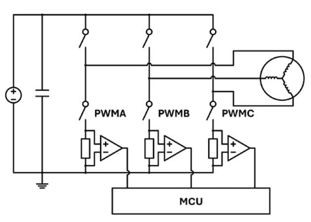
Figure 1. A three-phase inverter using threeshunt current sensing scheme. Image used courtesy of Bodo’s Power Systems [PDF]
Figure 1 shows an inverter circuit using a three-shunt current sensing scheme, where the phase currents are measured using shunt resistors. Amplifiers are then used to boost the sensing signals, allowing the use of low-resistance shunts to minimize power loss. The amplifiers also add a DC offset to ensure the signals stay within the MCU’s sampling range (typically 0–5 V or 0–3.3 V).
When a lowside switch is on, its corresponding shunt resistor carries the same current as the phase current. This enables accurate phase current measurement with properly timed ADC sampling. Figure 2 illustrates typical waveforms and ADC sampling points in a three-phase motor drive. The PWM signals are usually centre-aligned, and ADC sampling occurs at the midpoint of the on-state to minimize switching noise and accurately capture the phase current.
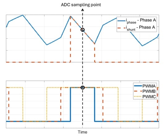
Figure 2. ADC sampling scheme for three-shunt current sensing. Image used courtesy of Bodo’s Power Systems [PDF]
Figure 3 shows the current sensing waveforms at each stage of signal processing, illustrating how the MCU reconstructs the phase current from the voltage signals across the shunt resistors. Bidirectional current sensing is essential for accurately measuring phase current in both directions, as demonstrated by the VCS waveforms.
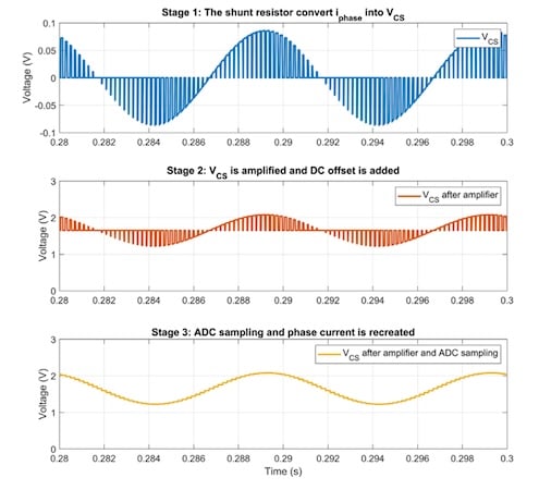
Figure 3. Signal processing stages for current sensing. Image used courtesy of Bodo’s Power Systems [PDF]
To reduce BOM cost and power loss, a two-shunt current sensing scheme can be used. This method measures only two of the threephase currents, with the third phase current calculated using (1).
ia + ib + ic = 0 (1)
Although the two-shunt current sensing scheme is more cost-effective and reduces power loss compared to the three shunt scheme, it compromises DC bus utilization. To increase the motor speed, the amplitude of the three-phase AC voltages from the inverter must be raised by increasing the modulation index. However, when the modulation index reaches one (i.e., full DC bus utilization), the duty cycle can drop to zero for certain periods, leaving no window for ADC sampling, as illustrated in Figure 4.
This limitation does not affect the three-shunt scheme because the missing phase current can still be calculated from the other two measured currents. However, in the two-shunt scheme, only one phase current remains known in this extreme case, leading to signal loss. To prevent this issue, the modulation index must be limited (e.g., to 0.8) to ensure an adequate ADC sampling window.
This restriction, however, reduces the maximum AC voltage output from the inverter and limits the maximum speed of motors as shown in Figure 5.
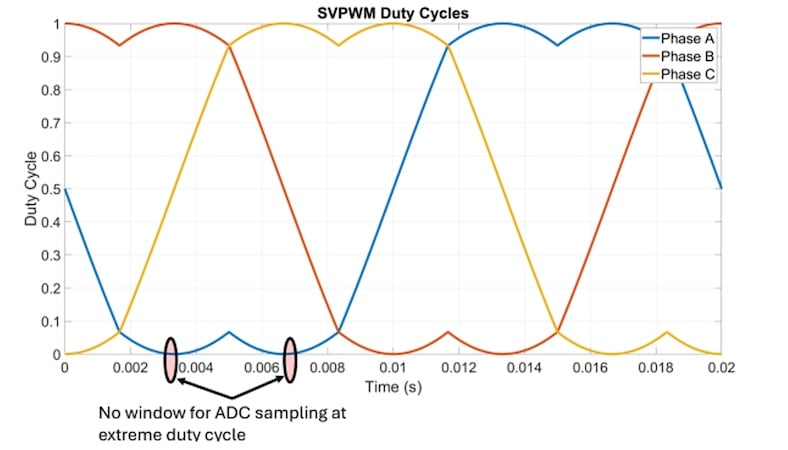
Figure 4. Duty cycles of Space Vector Modulation when modulation index = 1. Image used courtesy of Bodo’s Power Systems [PDF]
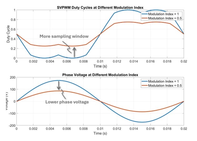
Figure 5. Comparison of duty cycles and phase voltage amplitudes under different modulation indices. Image used courtesy of Bodo’s Power Systems [PDF]
The system cost can be further reduced with a single-shunt current sensing scheme. Following the same fundamental principle as the two-shunt scheme, it requires more sophisticated control algorithms and introduces additional limitations due to the constrained sampling window.
Current Sensing with ICeGaN CS
Figure 6 shows the internal circuitry of the ICeGaN GaN IC from Cambridge GaN Devices (CGD) in order to explain how the current sensing works in this solution. The Main HEMT is the GaN HEMT that conducts the majority of the current. ICeGaN’s CS HEMT RDS(on) is much higher than that of the Main HEMT and is only used for current sensing.
The Main HEMT and CS HEMT’s gates are tied together such that they are on and off simultaneously. An external resistor RCS and the CS HEMT form a voltage divider, which measures the VDS across the device when the gate signal is high.
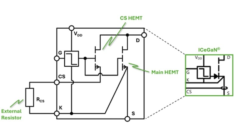
Figure 6. ICeGaN’s internal circuitry. Image used courtesy of Bodo’s Power Systems [PDF]
The CS pin output can be mathematically expressed by the following equations:
[
left{
begin{aligned}
V_{CS} &= 0 quad (text{Gate = low @ forward conduction}) \
V_{CS} &= frac{R_{CS} R_{ds,on_Main_HEMT}}{R_{CS} + R_{ds.on_CS_HEMT}} i_{D}
quad (text{Gate = high or diode conduction})
end{aligned}
right.
]
where VCS is the voltage across RCS, ID is the drain current, and Rds.on_Main_HEMT and Rds.on_CS_HEMT are the on-state resistance of the Main HEMT and CS HEMT, respectively. From the equations above, VCS is proportional to iD and hence can be used as the current sensing signal. Figure 7 shows an inverter circuit utilizing ICeGaN’s CS pins. It functions similarly to a three-shunt current sensing scheme but eliminates the need for costly shunt resistors, thereby reducing both component costs and power losses while enabling full DC bus utilization.
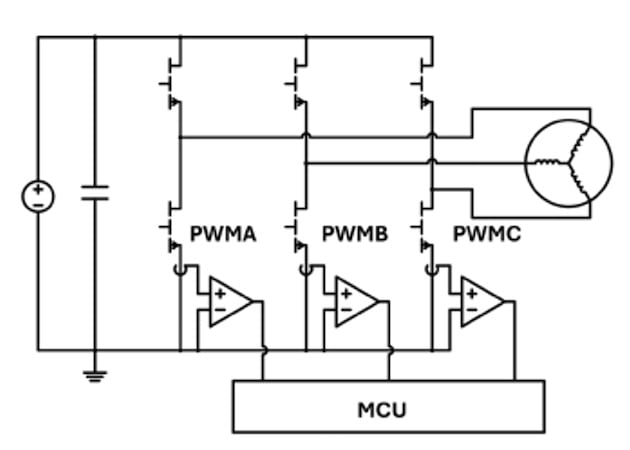
Figure 7. A three phase inverter using ICeGaNs lossless current sensing. Image used courtesy of Bodo’s Power Systems [PDF]
ICeGaN Current Sense Performance in a Three Phase Inverter
This section evaluates the ICeGaN CS performance in an actual three-phase inverter. The primary objectives of this evaluation are to assess the thermal performance of the inverter by using ICeGaN CS and to compare the final sensing output of ICeGaN CS with that of a shunt resistor after the amplifier stage. Two inverters were designed for the evaluation: one using three current shunts and the other using ICeGaN CS as shown in Figure 8.
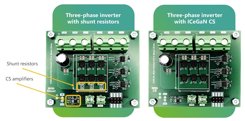
Figure 8. Inverter boards used to compare performance between ICEGaN CS and Three Shunt solutionBoth PCBs include an amplifier stage, allowing the final sensing output to be tested and compared. The key parameters are summarized in the table of figure 9. RCS is selected to be 7.5 Ω to provide the same sensitivity as the 0.1 Ω shunt resistor. Image used courtesy of Bodo’s Power Systems [PDF]
|
Parameters |
Three-phase Inverter with Shunt Resistors |
Three-phase Inverter with ICeGaN CS |
|
Amplifier Gain |
5 V |
5V |
|
Amplifier DC Offset |
1.65 V |
1.65 V |
|
RCS resistance |
N/A |
7.5Ω |
|
Shunt resistance |
0.1Ω |
N/A |
|
Switching Frequency |
15 kHz |
15 kHz |
|
GaN Device |
CGD65B240SH2 |
CGD65B240SH2 |
|
Modulation Method |
SVPWM |
SVPWM |
Figure 9. Key parameters for the 3-Phase Inverter Boards. Image used courtesy of Bodo’s Power Systems [PDF]
The current sensing performance at the negative peak is also compared in Figure 10. The ICeGaN CS output replicates the shunt resistor signal, demonstrating consistent current sensing performance.
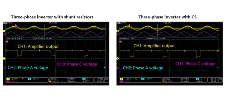
Figure 10. Comparison of CS amplifier output at the negative peak. Image used courtesy of Bodo’s Power Systems [PDF]
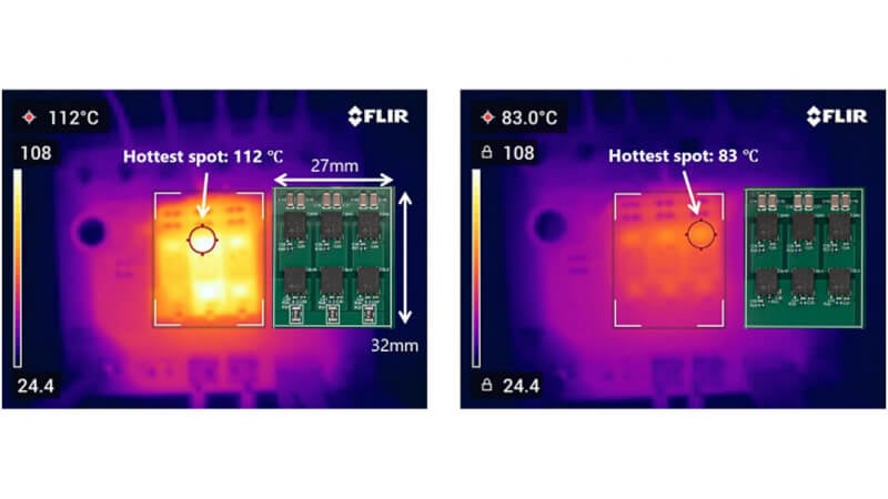
The thermal performance comparison is shown in Figure 11, demonstrating that the maximum case temperature is reduced by 29 K after eliminating the shunt resistors. The key factors contributing to this improvement are the reduced power loss from the shunt resistors as well as the low-side switches’ cooling pad, which can be extended to the ground plane.
Notably, the high-side switches, although not directly connected to or affected by the shunt resistors, also experience a significant temperature reduction. This is primarily due to the strong thermal coupling between devices in the inverter stage. As a result, eliminating the shunt resistors enhances not only the thermal performance of the low-side devices but also the overall inverter stage, making it a highly beneficial feature for motor drive applications.
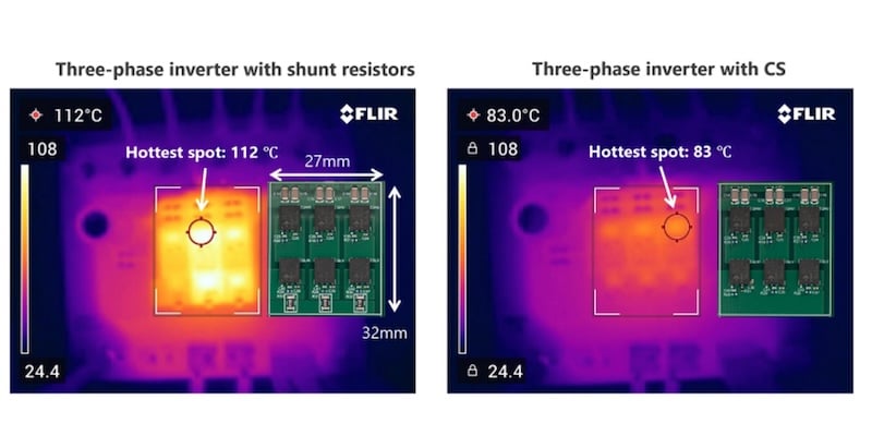
Figure 11. Comparison of thermal performance between the ICeGaN CS versus the 3 shunt. Image used courtesy of Bodo’s Power Systems [PDF]
Conclusion
ICeGaN devices are amongst the first GaN devices to integrate features such as an Integrated Miller Clamp and Lossless current sensing as well as the power HEMT in a true monolithic single die solution. A single die allows for simpler, smaller, and potentially more thermally efficient packaging, as there’s no need to co-package multiple chips with their own interconnects and wire bonds.
This translates directly to higher power density for the end product. Many so-called ‘integrated GaN’ solutions from other manufacturers, while offering ease of use, achieve this by co-packaging a silicon control/driver IC with a discrete GaN FET within the same package.
While this simplifies the system for the user, it introduces the complexities of two different semiconductor dies (GaN and Si) and their differing thermal and electrical characteristics, as well as the parasitics and reliability concerns of the interconnects between them. ICeGaN, by being truly monolithic, avoids these issues. Devices in a range of RDS(on) values are available now in production volume quantities.
This article originally appeared in Bodo’s Power Systems [PDF] magazine and is co-authored by Farhan Beg, Director of Application Engineering, and Huan Li, Regional Application Engineer, Cambridge GaN Devices (CGD)

